
“Ultra-Short-Reach Die-to-Die Link Design – Advanced Chiplet I/O Circuits” Online Course (2027)
Chiplets, advanced packaging, and high-bandwidth memory (HBM) are driving ultra-short-reach (USR) and die-to-die (D2D) links that span millimetres or centimetres yet deliver multiple terabits per second of aggregate bandwidth. Energy efficiency, bandwidth density, latency, signal integrity, and circuit area are therefore critical alongside per-lane data rate.
These links favour wide parallel interfaces, single-ended or ground-referenced signalling, modest channel loss, and forwarded-clock timing rather than the complex equalization and clock-recovery used in long-reach links. Their design requires understanding TX/RX circuits, package channels, timing, and advanced packaging. The course develops these concepts from first principles through practical circuit design and simulation.
USR system architectures, D2D interconnects, advanced 2D/2.5D/3D packaging, and key metrics including energy per bit, bandwidth density, data rate, and bit-error rate (BER) are introduced. We also examine how package technology affects the optimum electrical interface.
Package-channel behaviour is then covered, including insertion loss, reflections, inter-symbol interference (ISI), crosstalk, termination, and signal integrity. Single-ended, differential, ground-referenced, and simultaneous bi-directional signalling are compared in terms of pin efficiency, noise immunity, power, and circuit complexity.
TX and RX topics include voltage- and current-mode drivers, output impedance, termination, signal swing, TX equalization, amplification, sampling, offset, sensitivity, and continuous-time linear equalization (CTLE). The focus is on translating link specifications into circuit requirements and understanding how circuit choices interact with package-channel characteristics.
A dedicated session covers forwarded-clock link design, including multiphase clock generation, phase interpolators, clock distribution, lane-to-lane skew and de-skew, and timing calibration. The course examines source-synchronous timing and how timing budgets influence circuit and system design.
The final lecture focuses on HBM links, where extremely high aggregate bandwidth must be delivered under tight power, area, timing, and packaging constraints. Topics include HBM architecture, signalling, data and clock paths, timing relationships, channel characteristics, and circuit-design challenges as memory bandwidth and per-pin data rates increase.
Two real-world design projects emphasize practical design methodology and provide hands-on experience from specifications through circuit implementation and simulation. The first covers CTLE design from channel-loss specifications through transfer-function requirements, circuit design, transistor sizing, and simulation. The second focuses on TX and package-channel co-design, using link requirements to guide circuit-level decisions and evaluate performance.
Each lecture is accompanied by a homework assignment that reinforces key concepts through practical analysis and design. Assignments may involve hand calculations, circuit design, simulation, or MATLAB-based modelling, covering topics such as package-channel analysis, signalling comparisons, transmitter sizing, CTLE design, and forwarded-clock de-skew.
The course is intended for analog and mixed-signal IC, SerDes, I/O, and memory-interface designers, as well as engineers, graduate students, and researchers working on chiplets, advanced packaging, processors, accelerators, and HBM systems. Participants should have basic analog CMOS circuit-design and transistor-level simulation experience; familiarity with high-speed circuits, transmission lines, or SerDes is useful but not essential.
All Lectures @ 00:00-02:00 Beijing | 21:30-23:30 New Delhi | 16:00-18:00 Milan | 15:00-17:00 Dublin | 11:00-13:00 Boston | 08:00-10:00 San Diego
11th January 2027
Lecture #1 – Ultra-Short-Reach Links
Definitions, Applications, Architectures, Packaging, and Performance Metrics.
14th January 2027
Lecture #2 – Signalling and Package-Channel Modelling
Loss, Reflections, ISI, Crosstalk, and Signal Integrity, Single-Ended, Differential, Simultaneous Bi-Directional and Ground-Referenced Signalling.
18th January 2027
Lecture #3 – Transmitters
Driver Topologies, Relative Trade-Offs, Impedance Control, and Equalization.
21st January 2027
Lecture #4 – Receiver Front-Ends
Termination, Amplification, Sampling, Latch, Offset, and CTLE Fundamentals.
25th January 2027
Lecture #5 – Design Project #1: CTLE Design
From Channel-Loss Specification to Circuit Design, Simulation, Design Trade-Offs.
28th January 2027
Lecture #6 – Forwarded-Clock Link Design
Multiphase Generation, Phase Interpolators, Lane De-Skew, and Timing Calibration.
1st February 2027
Lecture #7 – HBM and Memory Links
Architecture, Signalling, Timing, Circuit, Thermal and Yield Challenges, Standard vs. Custom.
4th February 2027
Lecture #8 – Design Project #2: Transmitter and Package-Channel Co-Design
Single-Ended Signalling, Package-Channel Modelling, Reflections, Equalization, Driver Design, Eye Diagrams.
Duration: 16 hours
Format: 8 x 2-hour ‘Live-Virtual’ lectures (including Q&A), spread over 4-weeks. Attendance to the live lecture(s) is encouraged but not compulsory*.
Work: Homework assignments (optional) will consolidate the learning from the lectures.
Included:
- Course notes (PDF)
- Homework assignments (PDF)
- Lecture recordings* (up to 12 months playback access)
- Course homepage
- Class discussion forum (offline Q&A)
- Recommended reading list
- Extra material
- Attendance certificate
* Up to 12 months of on-demand access facilitates participants to revisit recorded sessions anytime or catch up at their own pace.
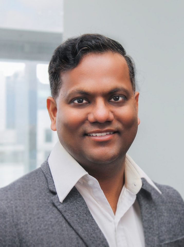
Sudip Shekhar is a Professor in the Department of Electrical and Computer Engineering at the University of British Columbia (UBC). Dr. Shekhar received his B.Tech. from the Indian Institute of Technology, Kharagpur, in 2003 and the MSc and PhD degrees from the University of Washington, in 2005 and 2008, respectively.
From 2008 to 2013, he worked as a Research Scientist in the Circuits Research Laboratory at Intel Corporation, Hillsboro, Oregon. He then joined the ECE department at UBC in 2013.
Dr. Shekhar is a recipient of the Schmidt Science Polymath Award, the UBC Killam Teaching Prize, the UBC Killam Award for Excellence in Mentorship, the Young Alumni Achiever Award by IIT Kharagpur, the IEEE Transactions on Circuit and Systems Darlington Best Paper Award, the IEEE Custom IC Conference (CICC) Best Overall Paper Award, the IEEE Radio-Frequency IC (RFIC) Symposium Best Student Paper Award, the European Conference on Optical Communications (ECOC) Best Student Paper Award, IEEE Solid-State Circuits Society (SSCS) Predoctoral Fellowship, the Intel Foundation Ph.D. Fellowship, and the Analog Devices Outstanding Student Designer Award.
He has served on the technical program committee of IEEE International Solid-State Circuits Conference (ISSCC), Optical Fibre Communication Conference (OFC) and CICC, and is currently the Tutorial Chair of ISSCC. He was previously a Distinguished Lecture of the SSCS Society.
His research interests include integrated circuits for high-speed interfaces, silicon photonics, radio-frequency transceivers and sensor interfaces.
Publications
Wireline Publications (Selected)
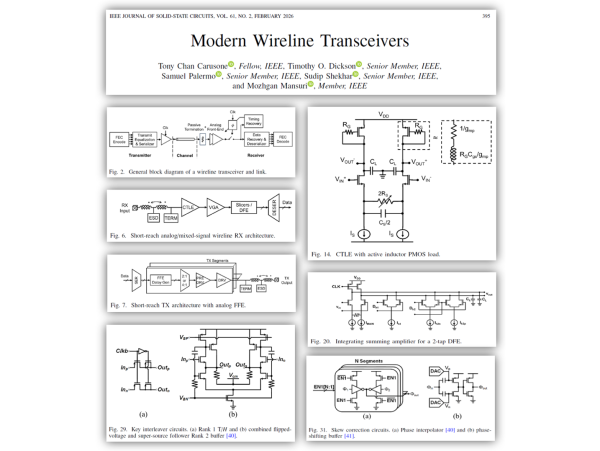
[2026] Modern Wireline Transceivers
[2023] Improving Linearity in CMOS Phase Interpolators
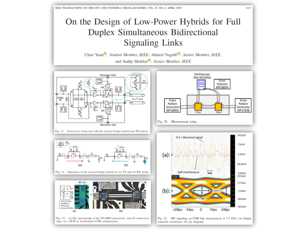
[2020] On the Design of Low-Power Hybrids for Full Duplex Simultaneous Bidirectional Signalling Links
[2018] A Type-I Sub-Sampling PLL With a 100×100μm2 Footprint and −255-dB FOM
[2015] A 0.5-to-0.75V, 3-to-8 Gbps/lane, 385-to-790 fJ/b, bi-directional, quad-lane forwarded-clock transceiver in 22nm CMOS
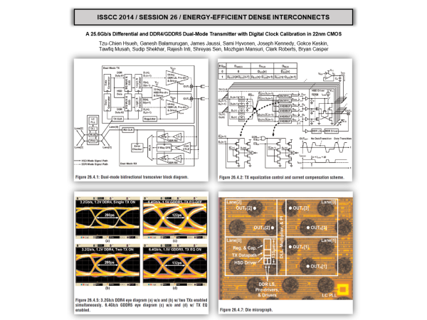
[2014] A 25.6Gb/s differential and DDR4/GDDR5 dual-mode transmitter with digital clock calibration in 22nm CMOS
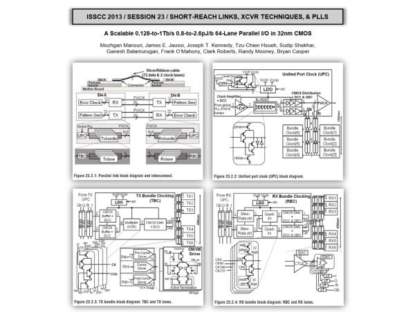
[2013] A scalable 0.128-to-1Tb/s 0.8-to-2.6pJ/b 64-lane parallel I/O in 32nm CMOS
[2013] Design considerations for low-power receiver front-end in high-speed data links
[2010] A 47x10Gb/s 1.4mW/(Gb/s) parallel interface in 45nm CMOS